Cathodoluminescence can be generated in the material when electron beam interacts with it. The technique has proven to be a probeless and contactless inspection with a broad spectral range.
But what are the necessary preparation steps that are needed to perform cathodoluminescence imaging? The sample preparation procedure is not difficult. In fact, the same steps are needed also to prepare the sample for general SEM imaging. Keep reading to learn more or watch our webinar on sample preparation for cathodoluminescence imaging.

Conductivity
You need to check whether the sample is conductive enough to prevent charging effects in the SEM. Charging is a standard issue that needs to be handled when working with SEM. This effect can be minimised by optimising beam parameters, such as energy and current. However, what needs to be taken into account is that lower energy and current might not be enough to excite the sample and get sufficient signal. Coating the sample with a thin layer of carbon or metal can be the solution. Then the coating layer will provide the conducting path for the charge.
High-vacuum compatibility
The sample has to be high-vacuum compatible: this needs to be taken into consideration when working with powders, samples that outgas, give out particles, or are wet. For some samples that are not conducting and can’t be coated, the Environmental SEM (ESEM) mode can be used. Cathodoluminescence imaging is compatible with this mode.
Stability under electron beam exposure
Even if the sample is stable in vacuum and is conducting, the interaction of the electron beam with the sample may cause damage because of heating, bond breaking or other effects. It is important to observe how the sample is behaving while imaging and to study these effects, to be able to trust the data.
Other steps
Make sure that the sample surface is flat enough: this can be achieved by polishing. Avoid large differences (> 0.1 mm) in height/surface roughness. If the surface is dirty, it can help to clean it chemically (e.g. isopropanol, acetone) or by reactive ion etching with oxygen, for example.
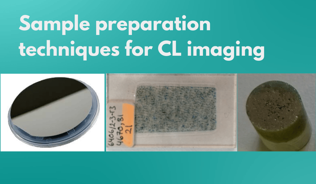
The most common preparation technique for geological materials is thin-sectioning (20 to 30 microns). Another way to prepare such naturally occurring samples is to embed them in resin.
Semiconductor wafers, an example of man-made materials, on the other hand, are normally flat and conducting already, so no additional preparation is needed in most cases. However, for all these materials, polishing can be very helpful to flatten the sample.
In addition to the materials mentioned above, it is also possible to look at materials in powder form. For this purpose, the powder can be put on a carbon tape to fix it, and be coated with carbon or metal if needed.
Learn more about the sample preparation process from our webinar below.
.svg "DELMIC")
.png)