.svg "DELMIC")
.png)


Fast electrons that are fired at a material cause it to become excited, thereby emitting photons of characteristic wavelengths. CL intensity measurement is one of the many useful methods using CL emission to obtain valuable information about your sample complementary to other techniques such as SE, BSE, EBSD or EDS.
This article further explains how CL intensity mapping exactly works and how it can be employed in various types of research.
To start with the basics: when an electron beam interacts with a material, a variety of processes occur which can be used for various kinds of microscopy. Aside from the well-known electron signals, a broad spectrum of electromagnetic radiation is generated. The radiation that is generated in the ultraviolet/visible/near-infrared regime of the electromagnetic spectrum is referred to as cathodoluminescence (CL). The electron beam causes the material to fluoresce as it returns to a ground state.
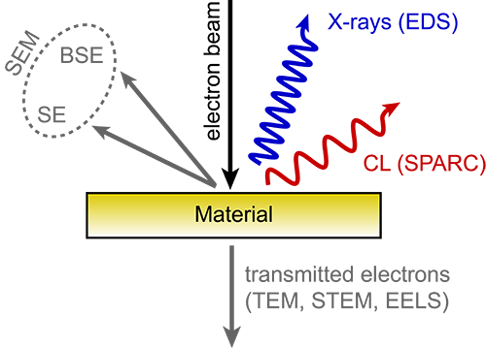
Figure: Schematic of the processes that occur when an energetic beam of electrons impinges on a sample. These processes are used for different characterization techniques as indicated in the schematic. CL is the electromagnetic radiation in the UV/VIS/IR spectral range.
Depending on your specific application, there are a variety of imaging modes and setups you can use to study cathodoluminescence signals. If you are interested in high-resolution EM imaging or combining EELS with CL, the best option to go for is STEM-CL. With STEM-CL, two advantages are: (1) the higher spatial resolution that can be achieved on your sample, and (2) the ability to combine with high resolution TEM imaging in-situ experiments. However, due to the small space available for inserting a mirror, the collection efficiency is rather low. Additionally, TEMs are often heavily booked and are a lot more complicated to operate compared to SEMs. Furthermore, the extensive sample preparation in STEM makes it possible in only a limited range of applications.
SEM-CL
SEM-CL is the better option for you if: you already own a SEM, you are interested in combining BSE, EBSD or EBIC with cathodoluminescence, or you don't want to go through the hassle of preparing your sample on a grid. Traditionally, SEM-CL can be divided in setups that allow hyperspectral imaging and setups that do panchromatic imaging or intensity mapping.
SEM-CL hyperspectral imaging
In hyperspectral imaging, a spectrometer is added to setup to obtain a spectrum at each point of the sample. Light coming from the mirror is focused on a slit or fiber connected to a Czerny-Turner spectrograph. A variety of imaging detectors can be used to cover a spectral range of 200-1600 nm. By scanning the e-beam across the sample, a spatially resolved hyperspectral image is produced.
The greatest advantage of using a spectrometer in your setup is the spectral resolution. The spectral resolution in commercial setups is typically around 1 nm, compared to 50 nm if you use panchromatic setups with filters. With the SPARC, another advantage is the ability to perform more advanced imaging such as angle resolved or polarimetry CL imaging which is enabled by the combination of an imaging spectrograph and camera.
The hyperspectral light-emission maps produced with CL illustrate the local density of electromagnetic states, a quantity that determines how well light couples to matter and vice versa. This makes the technique highly relevant to the field of nanophotonics. Disadvantages of spectral images, however, are (1) slow acquisition speed, and (2) the limited field of view. If you are measuring the CL signal with a spectrometer, the maximum scan speed is 10 ms per pixel. For example, if you are looking at zircons that are approximately 0.3-0.5 mm in size, it is very tedious to use spectral CL imaging. All light has to be focused through the narrow slit of the spectrometer, thereby greatly reducing the field of view. This small field of view thus makes it very difficult to scan your sample in one step.
SEM-CL intensity mapping
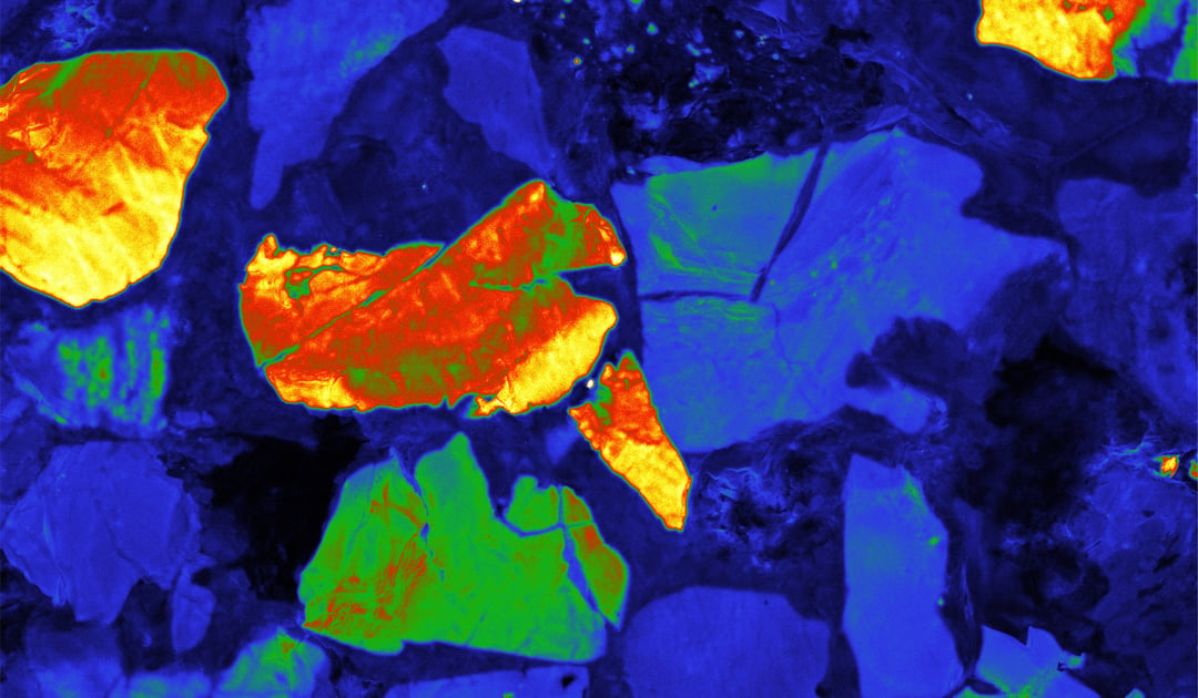
This brings us, finally, to intensity mapping. In intensity mapping, rather than using a spectrometer you are using a fast analog PMT detector. In this imaging mode you are not looking at the entire spectrum per pixel, but instead at the CL intensity of a pixel. In geology for instance, this CL intensity emission from a zircon gives insights into crystal growth, zonation, cementation, replacement, deformation, provenance, trace elements, and defect structures. This can be used to fingerprint rocks and reveal interesting spatial textures on a submicron scale.
Using a PMT detector for intensity mapping is done quickly: pixel times of 1 µs are easily attainable allowing video-rate scanning of materials making this method ideally suited for large-scale imaging and the rapid inspection of large areas. Another advantage of intensity mapping over hyperspectral imaging is the ability to scan a large field of view: contrary to hyperspectral imaging, the light does not have to be focused on the narrow slit of the spectrometer. These two characteristics make intensity mapping perfectly suited for geological applications, fast device inspection, and efficient region-of-interest finding.
After a broad inspection of the sample using panchromatic CL intensity mapping, a filter can be introduced for spectral differentiation. Of course, the spectral resolution of the setup including a filter wheel and PMT will never be as high as compared to hyperspectral imaging, but in many research fields this is not necessary as long as you use the right filters, as is the case for geoscience research.
Ultimately, there are several different ways of imaging cathodoluminescence emission from a sample. Depending on your sample and application, you have to make a selection of the setup and imaging mode that is best suited to your research.
If you are interested in reading more about intensity mapping click the link or image below to open our application note. If you're considering acquiring a CL setup suited for intensity mapping, have a look at our SPARC compact product.

Read CL intensity mapping application note
References
[1] Goodge, J. (n.d.) The Science Education Resource Center at Carleton College. Energy-Dispersive X-Ray Spectroscopy (EDS). Retrieved 6-9-2016 from http://serc.carleton.edu/research_education/geochemsheets/eds.html
[2] Chen, Z. Q., Yamamoto, S., Maekawa, M., Kawasuso, A., Yuan, X. L., & Sekiguchi, T. (2003). Postgrowth annealing of defects in ZnO studied by positron annihilation, x-ray diffraction, Rutherford backscattering, cathodoluminescence, and Hall measurements. Journal of applied physics,94(8), 4807-4812.
[3] Woods, G. S., & Lang, A. R. (1975). Cathodoluminescence, optical absorption and X-ray topographic studies of synthetic diamonds. Journal of Crystal Growth, 28(2), 215-226.

