.svg "DELMIC")
.png)


Thin-film solar cells made with this structure have received a lot of attention from the photovoltaics community for exhibiting conversion efficiencies of almost up to 23%.
Various microscopy techniques are commonly used to perform optoelectronic characterization of these highly relevant solar cell devices. These techniques include FIB-SEM investigations, for instance, which can help to investigate the high capability solar cells and do the material microstructure measurements. It is also quite common to use such techniques as electron backscatter diffraction, energy-dispersive X-ray spectrometry (EDX), electron-beam-induced current (EBIC).
One extremely powerful technique for analysing Cu(In,Ga)Se2 layers in high-efficiency solar cells is cathodoluminescence (CL). It is particularly useful for observing the Ga/In gradient and how it influences the optoelectronic properties of Cu(In,Ga)Se2 layers. It is possible to use energy-dispersive X-ray spectrometry to observe local-band-gap energies, but cathodoluminescence can be a more efficient technique for direct access of these local optoelectronic quantities.
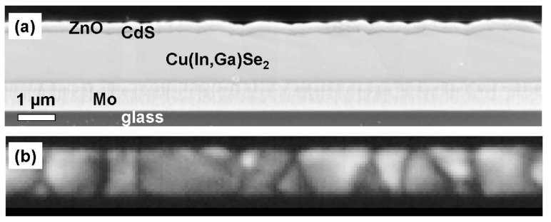
ZnO/CdS Cu(In,Ga)Se2/Mo/glass solar cell stack (Figure 1) was analysed with cathodoluminescence imaging at room temperature, and a CL spectrum was acquired in each pixel. While comparing the SEM and panchromatic CL images acquired on the same identical area it is possible to see that the CL intensity in neighbouring grains is different. These images also allow to conclude that the intensity is reduced at the grain boundaries due to enhanced nonradiative recombination.
Moreover, peak shifts in the CL map reveal the distribution of the local band-gap energy/wavelength well.
This experiment was performed by a research group from Helmholtz-Zentrum Berlin, which soon will host a workshop dedicated to studying photovoltaic materials with cathodoluminescence. The workshop will consist of several talks and hands-on sessions which will focus on the most relevant and advanced techniques for studying photovoltaic materials. The workshop is free and you can still register for it below.