.svg "DELMIC")
.png)


Nanophotonics is a rapidly expanding area of research that studies the behavior of light at the nanometer scale and the interaction of nanometer-scale objects with light. Nanoplasmonics, a subfield of nanophotonics, specifically focuses on the interaction between electromagnetic fields and conduction electrons within a metal. This interaction results in plasmons, which are coherent oscillations of the conducting electrons [1].
Nanoplasmonic materials can manipulate light below the optical diffraction limit. Furthermore, the plasmonic properties are tunable by modifying the composition and geometry of the material, and they also exhibit sensitivity to changes in the surrounding environment [2]. These characteristics make nanoplasmonic materials highly versatile and applicable in various fields such as [3]:
- Sensing
- Communication
- Lasers
- Optical displays
When excited, the nanoplasmonic material traps the light, which then propagates as a surface plasmon-polariton (SPP) or charge density wave, and subsequently scatters as light again. In confined places, energy can also be dissipated due to localized surface plasmon resonance (LSPR) [1].
The physics behind plasmonic oscillations
To effectively use plasmonic properties for various applications, it's crucial to have a precise understanding of how they harness and radiate light. Scanning electron microscopy (SEM) serves as a valuable tool for localized excitation at the nanoscale. Researchers commonly use electron energy loss spectroscopy (EELS) or cathodoluminescence (CL) imaging in an SEM to study the excitation of SPPs. However, interpreting EELS and CL data can be challenging [1].
To address this issue, Liu et al. developed an analytical electromagnetic model for the CL emission of a chemically-grown silver nanowire [1]. The aim of this model was to enhance our understanding of the physics behind different radiative processes and electron beam excitation in silver nanowires.
The researchers conducted two CL measurements on the nanowire. Firstly, they measured spectrally-resolved CL emission using Delmic’s SPARC Spectral detector. In this setup, a parabolic mirror collects the CL emission, which is subsequently focused on a spectrometer (Figure 1). Different pixels of the nanowire are excited by raster scanning the electron beam, and the emitted CL is collected for every excitation point. After the measurement, the spectrally-resolved CL emission is plotted as a function of the probe position.
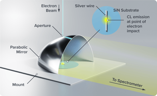
Figure 1: Setup to measure the spectrally-resolved CL emission with Delmic's SPARC Spectral CL detector. The electron beam goes through the aperture and hits the sample. The CL emission is then collected by the parabolic mirror and focused on the spectrometer.
Secondly, they measured spatially-resolved CL using Delmic’s SECOM, an optical fluorescence microscope mounted on an SEM. The CL emission from the nanowire is collected by the SECOM through a transparent substrate (Figure 2). By exciting at different points along the wire, the position of light emission, and relative intensity of the light can be measured. Similar to the previous measurement, the spatially-resolved CL emission is plotted as a function of probe position.
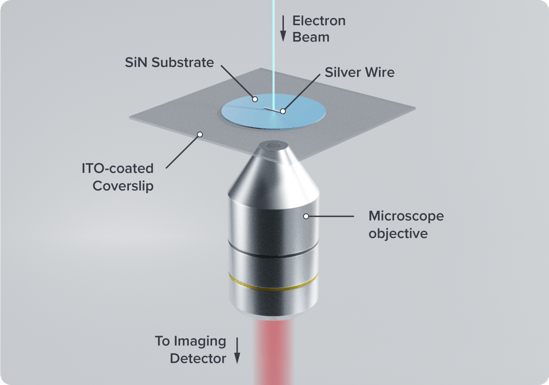
Figure 2: Setup to measure the spatially-resolved CL emission with Delmic's SECOM optical fluorescence microscope. The electron beam hits the sample and the CL emission goes through the SiN substrate. Subsequently, the microscope objective of the SECOM collects the CL emission.
Following these measurements, the researchers developed a simplified one-dimensional model to describe the interaction between the incident electron and the electric fields induced in the nanowire. They used this model to simulate the spectrally and spatially resolved CL measurements.
They found a good agreement between the CL emission plots obtained from the simulations and those obtained from the measurements. This model can thus be used to gain a deeper understanding of the physics involved in the interaction between electrons and surface plasmon excitations in a silver nanowire.
This scientific article demonstrates the application of cathodoluminescence imaging in an SEM to enhance the understanding of nanoplasmonic materials. It also presents an innovative method for conducting both spectrally and spatially-resolved CL experiments - using our CL detector and fluorescence microscope. We are excited to see even more ways in which our solutions can bring nanoscale insights in the future!
References
[1] Liu, A. C. Y. et al., Small, 2207747 (2023)
[2] Liz-Marzán, L. M. et al., Chem. Soc. Rev. 43, 3820-3822 (2014)
[3] Jiang, N. et al., Chem. Rev. 118, 6, 3054–3099 (2018)