.svg "DELMIC")
.png)


In the power industry, there is a growing demand for achieving ever-higher power densities and efficiency while simultaneously reducing power supply costs. As a result, silicon carbide (SiC) metal-oxide-semiconductor field-effect transistors (MOSFETs) have replaced other silicon-based technologies in numerous power applications due to their superior performance [1].
These SiC MOSFETs, available in the commercial market since 2011, enable high-density, efficient, and high-frequency power converter applications. Beyond Earth-based applications, SiC devices hold significant potential to be used in space as well [2].
However, space electronics are subjected to high amounts of radiation, so the radiation response of the SiC-powered devices had to be investigated. Research revealed that SiC-powered MOSFETs exhibit high sensitivity to energetic heavy ions, rendering them susceptible to single-event effects (SEE) and latent damages induced by radiation [2].
The reliability of SiC-powered MOSFETs depends on the operational drain-source bias Vds and on the linear energy transfer (LET) of the particle. In Figure 1, the different types of damage induced by heavy ions are summarized as a function of Vds and LET [3].
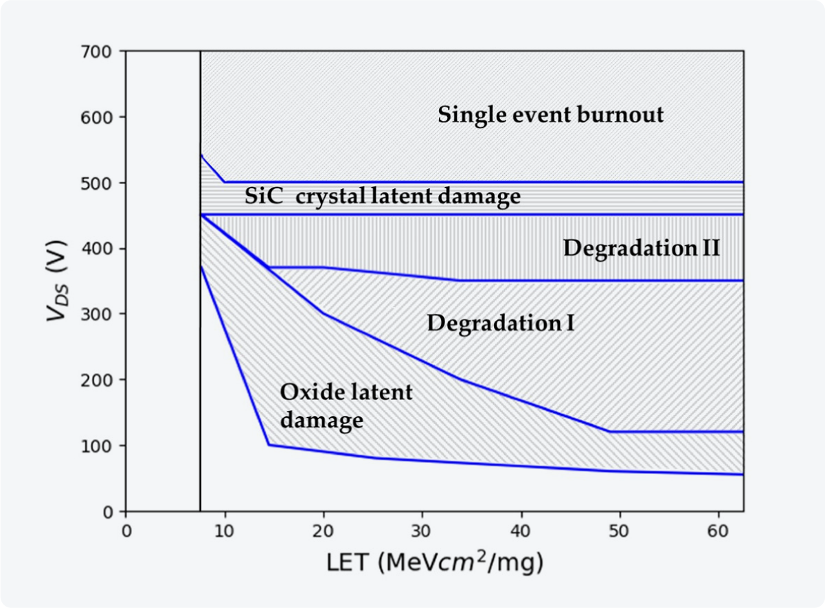 Figure 1: Types of damage induced by heavy ions in SiC-powered MOSFETs as a function of the operational drain-source bias (Vds ) and the linear energy transfer (LET) of the particle. Taken from [3].
As Vds surpasses the first threshold, latent damage occurs in the gate oxide, termed oxide latent damage. Upon further increase, there is a permanent rise in gate and drain leakage currents, which is referred to as degradation or ‘single event leakage current’ (SELC). SELC comprises two sub-regions, degradation I and degradation II. In degradation I, both drain and gate leakage currents increase equally, with the most sensitive area beneath the gate. In degradation II, an additional drain leakage current is observed in the p-n junction region, leading to permanent damage to the device.
While the types of degradation induced by heavy atoms are now identified, the precise mechanism behind the creation of these defects remains elusive. To address this gap of knowledge, Martinella et al. [4] investigated SELC effects in SiC-powered MOSFETs using cathodoluminescence spectroscopy. Cathodoluminescence (CL) is a valuable tool for measuring small-scale defects in SiC-powered MOSFETs.
Using CL, researchers can localize defect centers and identify common luminescence peaks.
The investigation into the degradation I and degradation II types was conducted using Delmic’s SPARC CL detector integrated into a scanning electron microscope (SEM).
Two devices were tested, with one undergoing SELC I degradation and the other undergoing SELC II degradation after irradiation. The researchers measured their CL emissions and hypothesized that bright CL signals would be caused by ion tracks, making the surrounding area of bright signals indicative of the extent of the damage that was being caused.
The investigation focused on the CL emission wavelengths of four different pixels (Figure 2). Pixel 1 and 3 emitted high-intensity CL signals, pixel 2 was selected as an intermediate signal and pixel 4 served as a reference for the background level. The device experiencing degradation type II appeared to have more extensive damage than type I.
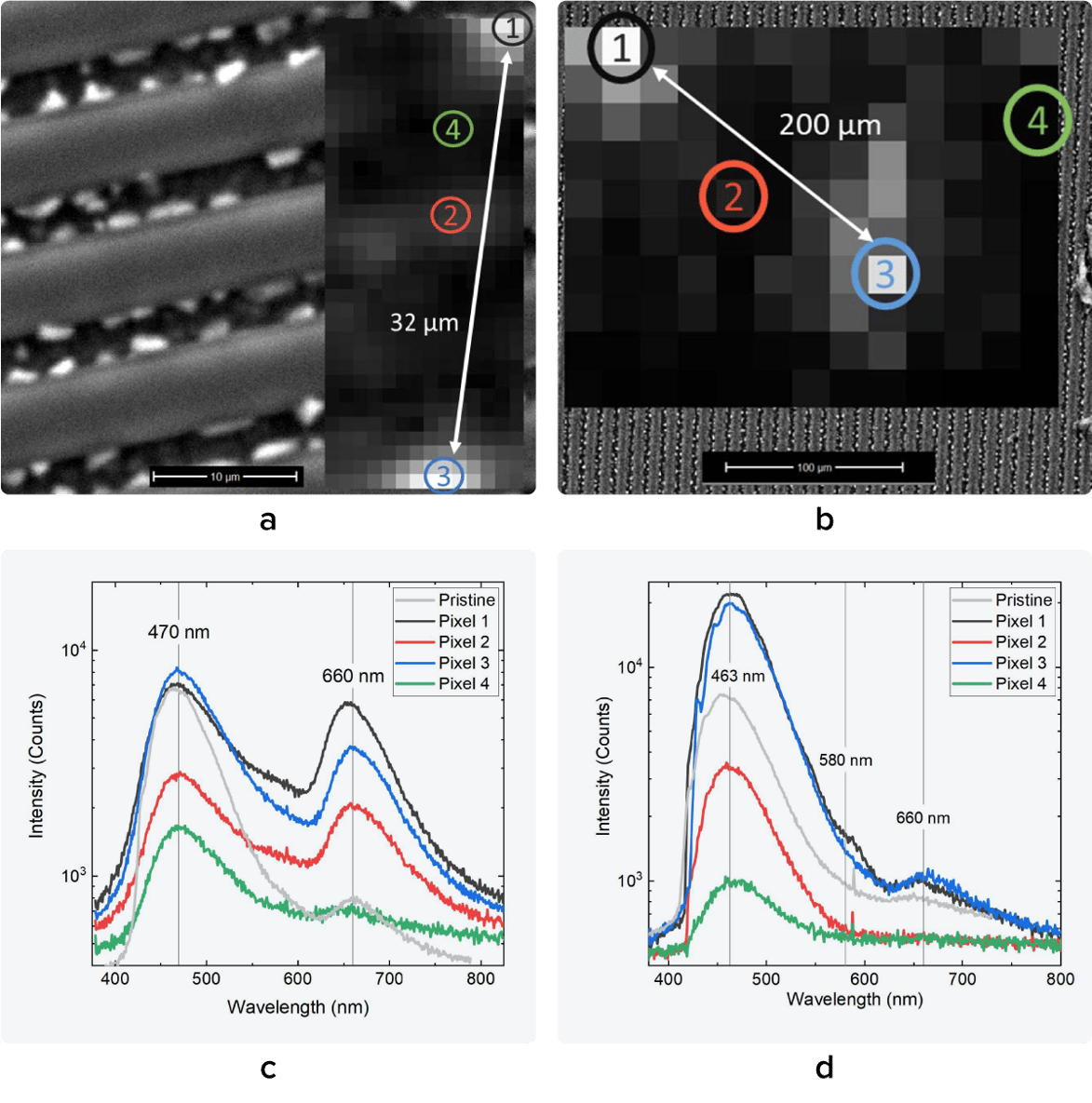 Figure 2 (a) and (b) show CL false color maps of the devices with SELC I and SELC II degradation respectively. Four pixels are investigated for each degradation type, indicated by the numbers. For each false color map, the CL spectrum as a function of the wavelength is plotted in (c) and (d) of the four pixels and a pristine reference. Taken from [4].
In the CL emission plots of the pixels, common luminescence peaks of defect centers from the thermal SiO2 were identified for both devices. Both spectra showed a peak at 455-480 nm, corresponding to oxygen vacancy centers (OVCs), and at 660 nm, representing non-bridging oxygen hole centers (NBOHCs). Only the device degraded with SELC II showed an additional peak at 580 nm, which is indicative of Si-N bonding structures.
When plotting additional CL signals from the device degraded with SELC I, the 580 nm peak was also identified, but with a similar intensity as the OVC and NBOHC peaks.
This research marks the first step in identifying the defects of SiC-powered MOSFETs caused by irradiation.
The researchers showed that cathodoluminescence is a valuable tool in defect identification. Further research can validate the identification of these defects and establish connections with the performance degradation of the devices. A better understanding of the defects in these MOSFETs could pave the way for a solution to this phenomenon. This could enable space electronics to follow the path of the power industry, achieving higher power densities and efficiencies and enabling powerful new applications.
References
[1] Wang, J. et al., IET Power Electronics, 13, 445-455 (2020)
[2] Galloway, K. F. et al., Reliability Concerns for Flying SiC Power MOSFETs in Space (No. GSFC-E-DAA-TN65899), (2018)
[3] Martinella, C. et al., Microelectronics Reliability 128, 114423 (2020)
[4] Martinella C. et al., Materials Science Forum 1090, 179–184 (2023)