.svg "DELMIC")
.png)


It is used to probe important material properties such as the local band edge emission, local defect band emission, point defects, and delocalized defects. It also allows measuring damage and strain to the material, dopant distribution, and carrier diffusion. These characteristics of semiconductor materials are very important for industrial applications.
So what makes cathodoluminescence imaging such a beneficial technique?
Unlike other near-field inspection techniques, cathodoluminescence is probeless and contactless. Since the electron beam is a broadband excitation source, it is possible to inspect the complete spectral range of the sample, all the way from the deep UV to the infrared. The excitation resolution is nanoscale, as it is only determined by the electron excitation process. Additionally, the electron penetration depth is tunable: by changing the energy of the electron beam, you can perform depth-resolved studies and image buried structures in materials. Finally, fast scanning is enabled by scanning electron microscope (SEM) as well as correlation with other imaging modalities, including SE, BSE, EDS, and EBSD.

Which application fields can it be used for?
Cathodoluminescence imaging can be used to study:
- Solid-state lighting and displays
- Power electronics, which are made using solid-state devices such as semiconductor diodes and power transistors
- Photovoltaics
- Laser diodes and VCSELs (vertical cavity surface emitting lasers)
If you are working with semiconductors, CL can play an important role in quality assurance and metrology, failure and defect analysis, materials and device development, and R&D applications.
CL data provides information on the composition, crystal structure, any trace elements and dopants present, crystal defects, and ionization state.
How can CL imaging be performed?
Depending on the configuration of the cathodoluminescence detector, various imaging modes are available for studying semiconductor materials.
In cathodoluminescence intensity mapping, the electron beam raster scans the sample, and the CL is collected for every pixel. The advantage of this mode is that the sample can be scanned very fast: this is particularly helpful when you need to decide what you would like to image in more detail. Moreover, a large field of view can be scanned, which is useful for large semiconductor samples.
Another powerful imaging mode is hyperspectral imaging or spectroscopy. Using this mode is most beneficial when a full spectrum for different excitation positions is needed. The benefit of this mode is that this high spectral resolution data can be used for in-depth materials analysis.
Angle-resolved imaging, another imaging mode, is used to measure the directionality of light emission. The main benefit of this mode is the high angular resolution and a large numerical aperture covered in one shot.
Finally, with CL you can perform lifetime measurements and observe how the photons emitted from a source are distributed in time.
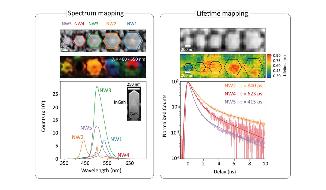
Image: Hyperspectral and time-resolved decay trace CL data from InGaN nanorods. Images courtesy of S. Meuret (AMOLF).