.svg "DELMIC")
.png)


Silicon is the most common semiconductor material thanks to its ease of availability, and has found widespread commercial applications. However, silicon being an indirect bandgap material, has several limitations that restrict its application. Compound semiconductors, a better-performing type of semiconductor, were discovered 17 years ago. They consist of chemical elements of two or more species, often providing higher processing speed and more favorable optoelectronic properties than silicon.
They have lower thermal noise at room temperature, can be operated at higher temperatures, and their band gap can be tuned by alloying in different compositions, to enable selection of the emission wavelength. Compound semiconductors can be found in power amplifiers for smartphones and other wireless devices, as well as in light sources for DVDs, Blu-rays, LEDs, and solar batteries. The main barrier for the commercial development of compound semiconductors is, however, that they are more expensive to process.
 Example of a CPU which is made of million tiny transistors (Source: Krbo|Flickr)
Gallium Nitride (GaN) is one of the most common compound semiconductors, which can conduct electrons 1000 times more efficiently than silicon while operating at a lower voltage. Because of their ability to assist high-speed switching, GaN and other compound semiconductors are being used in key markets like photonics and optical and RF communication. The development of compound semiconductors could benefit various technologies like safety systems, aerospace, and automotive applications, that demand high-performance levels along with sensing. Therefore, research in the field of compound semiconductors is a hot topic in academia as well as in industry.
Cathodoluminescence (CL) imaging, the perfect tool to study (compound) semiconductors
CL imaging and spectroscopy are used extensively to study GaN materials and devices. The SPARC is a high-performance cathodoluminescence detection system. With a one-of-a-kind high-precision mirror stage, the SPARC opens new avenues for research into semiconductors and compound semiconductors such as GaN-based LED materials. An energetic electron beams excites the wide bandgap (3.4 eV) of GaN efficiently with subwavelength spatial resolution. The emitted light is used to image local defects such as dislocations and to probe light emission characteristics on small length scales. As LED devices become increasingly miniaturized, cathodoluminescence serves as the most important tool for examining them at the nanoscale. Furthermore, by varying the energy of the primary electrons, different depths can be probed, thus allowing one to obtain more information in the case of stratified devices. Delmic has also published an application note on Cathodoluminescence for bulk and nanostructured Gallium Nitride-based LED materials.
Fully understand the complex 3D semiconductor structure using time-resolved CL imaging
Together with the SPARC, the LAB Cube, which is a module for time-resolved cathodoluminescence imaging, can be used to study the time dynamics of various materials, including semiconductors. This module allows performing lifetime imaging and g(2) imaging, including anti-bunching experiments, and it is a great tool for providing insights into intrinsic material properties, nanoscale quality and defects. It is highly relevant for a large range of applications including compound semiconductors for optoelectronic devices such as (In)GaN, perovskites, and GaAs. The LAB Cube module is a unique and easy-to-use system, which can be retrofitted on any Scanning Electron Microscopy and with the SPARC system without any extra modification.
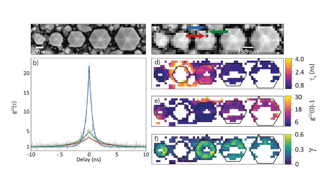
The figure below shows an example of a g(2) measurement on an array of GaN nanorods with InGaN quantum wells inside. In this case, the electron beam is raster-scanned over the array and for each position, a g(2) curve is acquired. The bunching effect can be clearly seen in (b) where g(2)(0) is clearly larger than 1. For every scanned pixel, the bunching peak is used to extract the local lifetime τe and excitation probability γ.
 Example of g(2) mapping data on InGaN/GaN nanorods shown in the SEM image in (a). (b) The g(2) data recorded at three colored squares as indicated by the arrows in panel (c) which shows SE intensity recorded together with the g(2) data set. Maps of (d) lifetime τe, (e) amplitude g(2)(0)-1, and (f) the probability of excitation γ are also shown. If the data was too noisy to extract these parameters, the pixel was left white in the map The contours of the nanorods are indicated by the black lines. Figure courtesy of Dr. Sophie Meuret (AMOLF, Amsterdam)
This information gained from imaging the dynamics of the semiconductor with the SPARC can be used to understand and quantify electron beam interaction with such a complex 3D semiconductor structure and to provide insight into the quality and homogeneity of the material.
If you are interested in our product – the LAB Cube, please download the Product sheet for more information.
For more possibilities about the SPARC system and the Lab Cube, do not hesitate to contact us or request a quote.

