.svg "DELMIC")
.png)


Currently, the standard display screens used are liquid-crystal displays (LCDs). LCD screens generate light by using a backlight, and the light is modulated by liquid crystals combined with color filters, forming individual subpixels. This design is quite inefficient, with only 5-10% of light being effectively used [1].
In contrast, OLED displays consist of organic subpixels that act as their own light emitter eliminating the need for an LCD element in the screen (Figure 1). This allows for individual control of brightness and the screens can be made flexible or even foldable. OLED technology also eliminates light leakage, which improves overall efficiency. However, some significant issues still need to be improved, such as burn-in and short lifetime [2]
MicroLED (µLED) displays are similar to OLEDs and thus have the same advantages, but instead of relying on organic material to emit light, they use robust inorganic materials such as InGaN and AlGaInP. These materials are already used in LED technology for ambient lighting and automotive applications [1][3]. In theory, MicroLEDs offer additional advantages, including:
- Smaller pixel size
- Significantly brighter pixels
- Longer lifetime
- Greater environmental stability
- Higher energy efficiency
- Faster response times
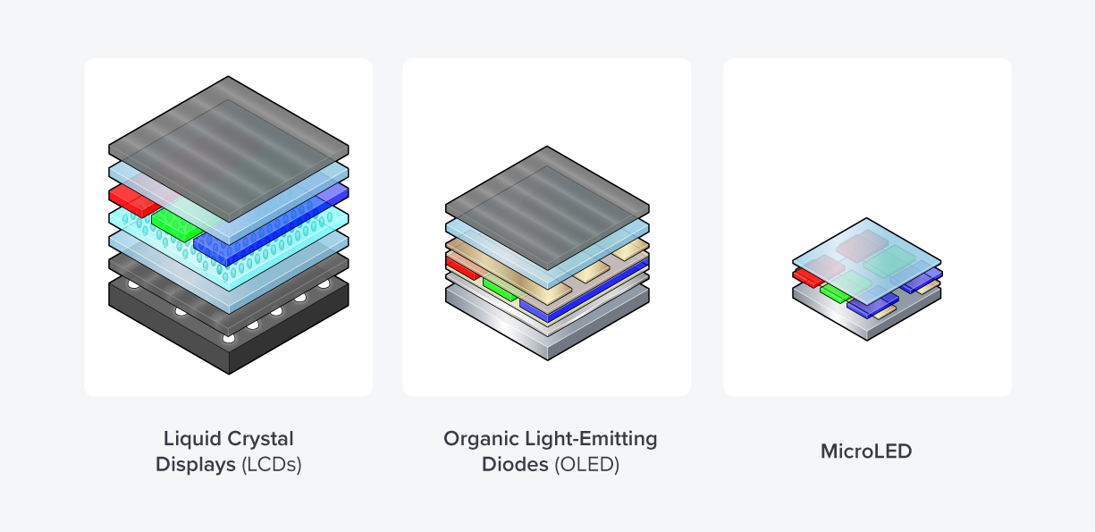 Figure 1: Schematic representation of the layered structure of LCD, OLED, and microLED screens. LCDs consist of a backlight module, a polarizer, a glass substrate, a liquid crystal solution, a color filter, a glass substrate, and a polarizer. OLEDs consist of a substrate, an electrode, an HTL/HIL layer, an organic light-emitting layer, an EIL/ETL layer, an electrode, an encapsulation layer, and a polarizer. In contrast, microLEDs have a simplified structure with only four layers, namely a substrate, an electrode, an RGB microLED, and a film or glass. The layers are listed in the order from bottom to top.
The smaller pixel size is particularly beneficial for displays viewed up close, where a highly immersive experience requires a very high pixel density.
This is the case with applications such as virtual reality (VR), augmented reality (AR), and to a lesser extent smartwatches and smartphones (Figure 2). For larger display screens viewed from a distance, such high pixel density is unnecessary and very costly. An alternative for these larger screens is using miniLEDs, which do not provide pixel-level dimming, but are easier to manufacture than microLEDs, and have a higher dynamic range compared to LCD due to their increased brightness [2][4].
 Figure 2: Oculus VR headset. These headsets currently have LCD or OLED screens. MicroLED technology could significantly improve the immersive experience of these headsets.
The biggest challenges with microLED technology lie in their manufacturing process and their small-scale defects. Currently, microLED displays have lower efficiency, higher power consumption, and considerably high costs compared to OLED and LCD displays [3]. Below, we will discuss the main challenges associated with microLEDs and potential solutions.
MicroLED manufacturing and defects hamper commercialization
The production process of microLED displays typically involves producing the LEDs on a wafer and then transferring them onto a backplane. The main difficulty lies in hybridizing the microLED wafer into the backplane. Several companies are working on innovative solutions to streamline this process [3].
Ideally, the LEDs would be directly grown onto the backplane, a technique known as monolithic integration. Researchers in the semiconductor field are actively working on this approach, especially since the recent incorporation of the More than Moore concept in the semiconductor industry roadmap. However, monolithic integration faces numerous challenges that are not expected to be resolved in the near future [5].
Consequently, an alternative approach called ‘pick-and-place transfer’ has been developed. In this method, the red, green, and blue LEDs are usually picked from the growth substrate using a transfer medium, the pitch size is adjusted, and they are aligned and individually moved to a backplane (Figure 3) [6]. Currently, pick-and-place is time-consuming, contributing to the high costs of microLED screens.
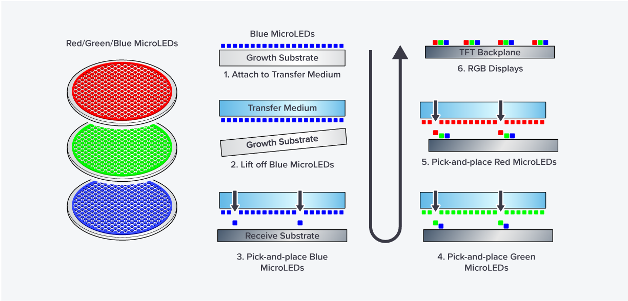
Figure 3: The general 'pick-and-place' transfer method for RGB microLEDs. The RGB microLEDs are grown on separate growth substrates, attached to a transfer medium, and individually placed on one TFT backplane. Taken from [6].
Another issue arises from the likelihood of defects occurring during the picking and placing of millions of microLEDs. When it comes to display screens, very close to 100% yield is expected, making defects or missing pixels unacceptable [6]. Mass-transfer techniques are being developed to increase the throughput and transfer accuracy and to make the process more cost-efficient [6].
Furthermore, there is an inherent challenge related to the microLEDs themselves. Defects on the side walls can lead to lower external quantum efficiency (EQE) in LEDs. This issue becomes significant when scaling down the LEDs to microLEDs. Therefore, although microLEDs have higher efficiency in theory, in practice the sidewall defects result in lower efficiency compared to established technologies [1].
Therefore, researchers are actively working on enhancing the microLED design to get rid of sidewall defects.
New microLED structures and designs are explored, as well as process improvement and the use of quantum wells (QWs) for RGB color conversion, and nanowires with 3D LED designs [1][7][8]. In a particular study, researchers investigate a novel approach to enhance efficiency and minimize defects in InGaN micro-LEDs with QWs for red color conversion [9]. They use a six-sided InGaN pyramid and compare two methods for reshaping the pyramids into flat microLEDs, namely high-temperature annealing and chemical mechanical polishing (CMP) (Figure 4).
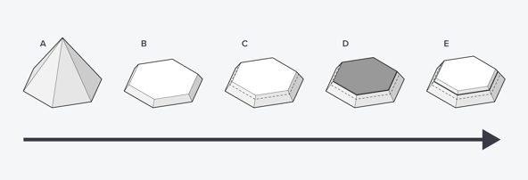 Figure 4: Illustration of the growth steps to reshape a six-sided pyramid into a microLED. A) A hexagonal pyramid is grown. B) The tip of the pyramid is removed to flatten the structure using either high-temperature annealing or chemical mechanical polishing. C) A second layer is grown to ensure a flat top surface for QW growth. D) The QW is grown on top. E) A top barrier is grown with the same composition as the lower barrier. Adjusted from [9].
To identify the occurrence of inhomogeneities during the microLED growing process, the researchers used hyperspectral cathodoluminescence (CL) imaging, which reveals emission variations for each pixel. They could successfully create red InGaN microLEDs and found that only the CMP flattening method does not damage the microLED structure. Although these designs are still in the experimental phase, they have the potential to improve the cost-efficiency and yield of microLED technology.
It is thus clear that microLED technology could revolutionize the display industry, and enhance the immersive experience of VR and AR technologies. However, the difficult manufacturing process and sidewall defects currently hamper the commercialization of this technology. A lot of research is therefore conducted to enhance the microLED efficiency and to make it more cost-efficient.
Despite these challenges, Apple has announced its plans to release a micro OLED AR headset called Apple Vision Pro in 2024 [10]. As the microLED technology is expected to develop further and become more scalable, we might be able to buy more affordable microLED AR/VR headsets sooner than we think.
References
[1] Webinar MicroLED displays (Yole group)
[2] Huang, Y. et al., Light Sci Appl 9, 105 (2020)
[3] Chen, Z. et al., J. Phys. D: Appl. Phys. 54, 123001 (2021)
[4] Wu, T. et al., Applied Sciences 8, 9, 1557 (2018)
[5] Cheng, Y. et al., Integration 85, 97-107 (2022)
[6] Chen, F. et al., Int. J. Extrem. Manuf., 4, 042005 (2022)
[7] Chen P.-W. et al., IEEE Photonics Journal 12, 4, 1-11 (2020)
[8] Liu, X. et al., Photon. Res. 10, 587-593 (2022)
[9] Gustafsson, A. et al., Nano Ex. 2, 014006 (2021)
[10] Apple Vision Pro headset press release