.svg "DELMIC")
.png)


Over the past 50 years, the semiconductor industry has transformed technology by exponentially reducing the size of silicon chips. This was made possible by following a roadmap based on Moore's law since 1970, which led to the doubling of the number of components per integrated circuit every two years. As a consequence, chips have become smaller and faster, and manufacturing has become cheaper.
However, the trend to miniaturize components couldn’t continue indefinitely due to quantum uncertainties [1]. Even before reaching this limit, other problems arose. By making the components smaller and faster, the integrated circuit would get too hot.
As a result, experts stated that Moore’s law was dead and that the industry had to adopt a new roadmap. Therefore, in 2016 the International Roadmap for Devices and Systems (IRDS) was introduced. The latest updated IRDS includes thirteen international focus teams (IFTs), two of which are named ‘More Moore’ and ‘More than Moore’ [2]. In this blog post, we will focus on these two IFTs and their various applications.
Building upon Moore’s law
Instead of completely discarding Moore's law, a whitepaper in 2005 explored the possibility of building upon it [3]. The authors recognized the need for advancements in both digital and non-digital functions within an integrated system. Most microelectronic devices consist of integrated circuits with digital components, including CMOS transistors and storage units, as well as non-digital components on a printed circuit board. The authors suggested that progress could be achieved by improving the digital components and integrating non-digital components into the integrated circuit. This led to the development of the concepts 'More Moore' and 'More than Moore' (Figure 1).
More Moore is the continuation of Moore’s law. It aims to scale down the transistor size and increase the number of components per integrated circuit while maintaining or improving performance. Research in this area has focused on exploring new technologies such as two-dimensional semiconductor materials, and stacking components such as transistors vertically [4][5][6].
More than Moore is the functional diversification of the integrated circuit. It focuses on integrating new materials and functionalities on the chip by incorporating non-digital components. This includes interaction with the outside world through sensors, and powering the product. More than Moore is not an alternative to Moore’s law, but an addition to the system that could create higher value systems [3]. These systems are designed with a certain application field in mind and enhanced by making targeted and application-based improvements.
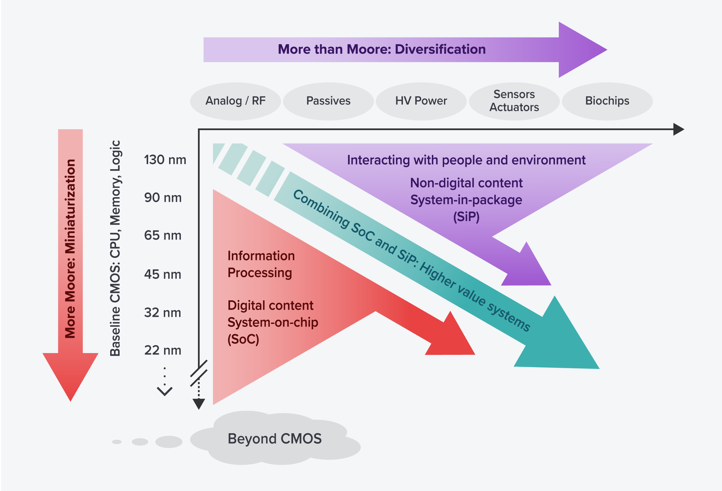
Figure 1: The concepts of More Moore and More than Moore. Higher value systems can be created by focusing on both miniaturization and diversification by adding non-digital content to the systems. Taken from [3].
More than Moore devices
The incorporation of the More than Moore law in the semiconductor industry roadmap has resulted in the development of More than Moore (MtM) devices. These devices are specifically designed for various application fields such as the automotive, telecom, entertainment, and clean energy industries, and there is a growing demand for their wafers (Figure 2) [7]. For instance, in the automotive industry, micro-electro-mechanical systems (MEMS) sensors are widely adopted due to their reliability and cost-effectiveness [8]. Another notable development is the improvement of solar cells using perovskite material, which results in enhanced efficiency [9].
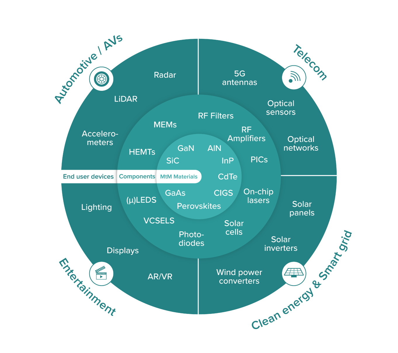
Figure 2: Main application fields for the More than Moore (MtM) devices. In the center, various MtM materials can be seen, further outward MtM components and end-user devices can be seen for the four application fields.
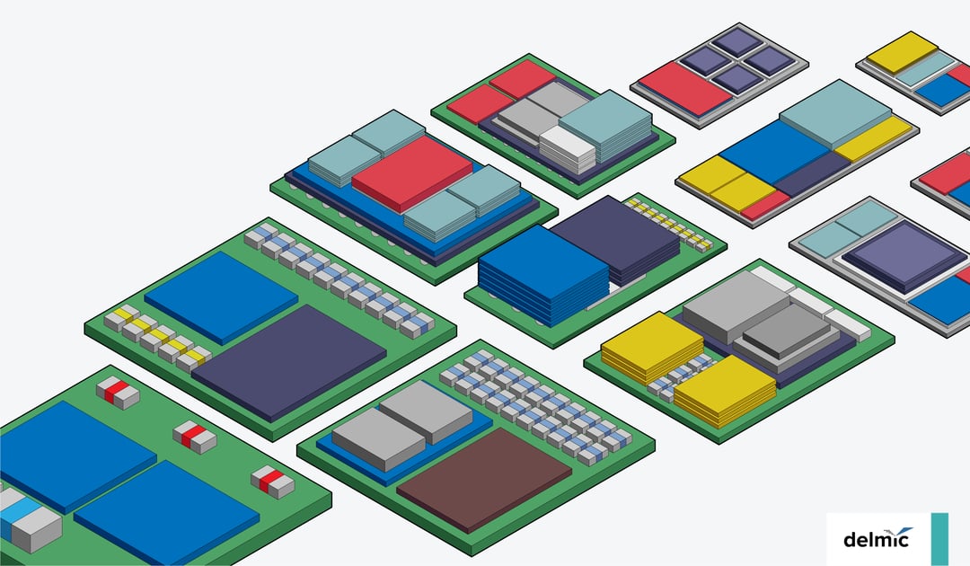
Additionally, there have been advancements in the development of photonic integrated circuits (PICs). These functional circuits use light instead of electrons, which are used in electronic integrated circuits. PICs can be used for optical telecommunication, offering advantages such as no interference from EM, higher bandwidths, and lower losses compared to electromagnetic systems. Generally, PICs consist of light emitters (lasers and LEDs), detectors, and modulators that enable the detection, generation, and transportation of light (Figure 3).
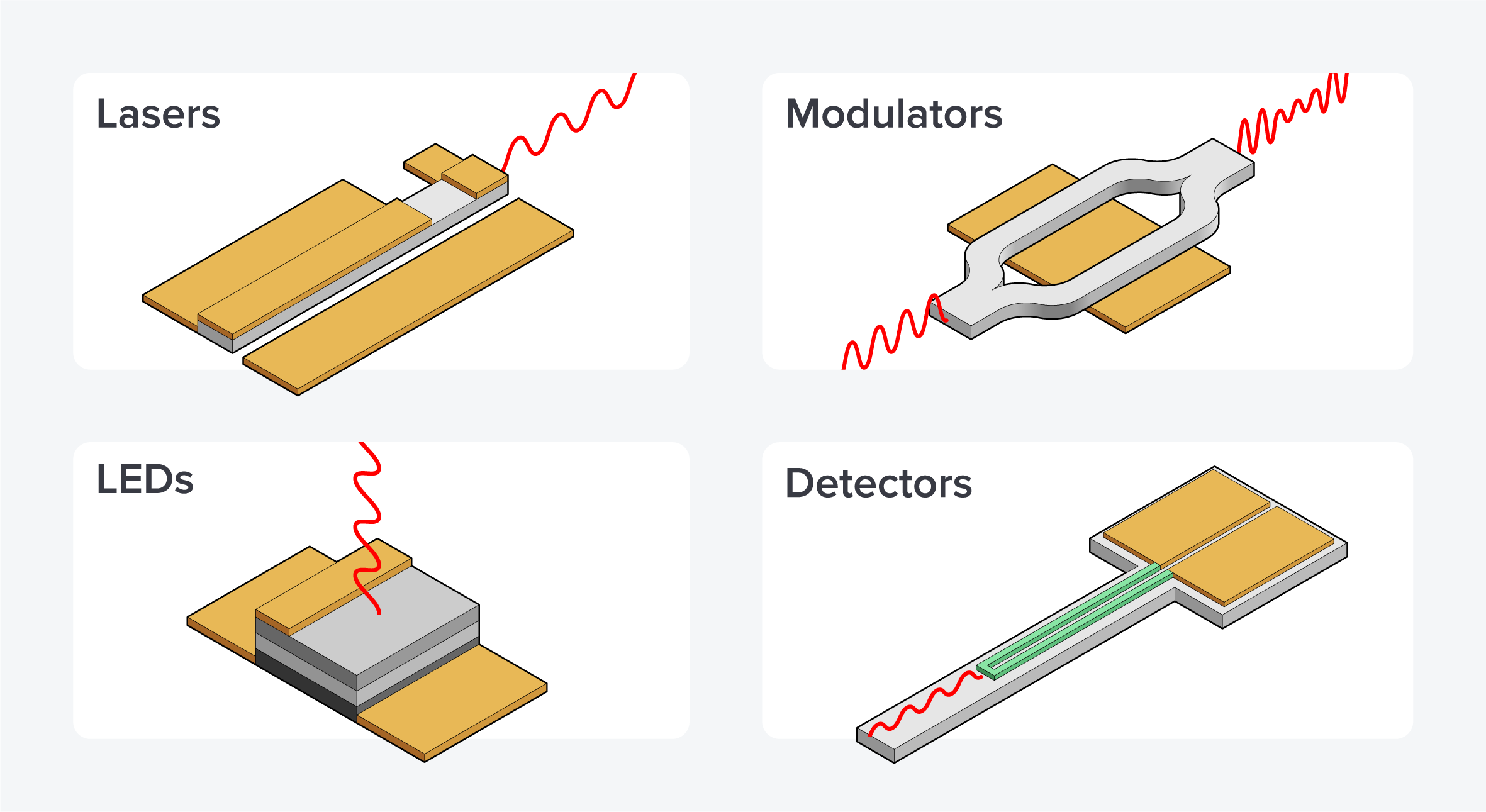
Figure 3: Standard photonic integrated circuit (PIC) components. PICs usually consist of detectors, modulators, and lasers or LEDs.
Researchers are striving to reduce the size of PIC components and achieve monolithic integration on silicon. Monolithic integration could improve the reliability and power consumption of the system, as well as reduce packaging costs and fiber coupling loss [10]. However, because of complexities in materials growth, substantial efforts are also put into heterogeneous integration approaches where different components are integrated into a single high-level assembly [11].
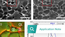
To address these challenges, various material platforms are being developed including silicon and silicon nitride for the photonic waveguide elements, and III-V semiconductor materials for light sources and detectors [12]. The III-V semiconductors are based on materials such as gallium nitride (GaN) and indium phosphide (InP) [10][13][14]. Research has mainly focused on improving material quality and efficiency. By using techniques such as cathodoluminescence imaging, nanoscale defects in such materials can be detected to optimize the properties of these materials [15][16].
The semiconductor industry’s roadmap has thus evolved beyond Moore’s law, now encompassing the concepts of More Moore and More than Moore. This shift has created exciting opportunities for research into the development of application-specific chips such as PICs, and will drive significant advancements across various fields.
References
[1] Waldrop, M., Nature 530, 7589, 144+, Gale OneFile: Health and Medicine, (2016)
[2] International Roadmap for Devices and Systems
[3] Arden, W. et al. "More-than-Moore white paper." Version 2, 14 (2010)
[4] Liu, Y. et al., Nature 591, 43–53 (2021)
[5] Tianyao Wei, T. et al., Science 25, 10, 105160 (2022)
[6] Tayal, S. et al. Silicon 14, 3543–3550 (2022)
[7] Blog post ‘More than Moore Devices: The Wind of Change’
[8] Basu, A.K. et al., Sensors for Automotive and Aerospace Applications. Energy, Environment, and Sustainability. Springer (2018)
[9] Kim, J.Y. et al., Chem. Rev. 120, 15, 7867–7918 (2020)
[10] Coldren, L.A. et al., Journal of Lightwave Technology 29, 4, 554-570 (2011)
[11] Heterogeneous Integration Roadmap
[12] Shibnath Pathak, Chapter 7 - Photonics Integrated Circuits, In Advanced Nanomaterials, Nanoelectronics, Elsevier, 219-270 (2019)
[13] Cai, W. et al, J. Micromech. Microeng. 28, 065003 (2018)
[14] Zhao, H. et al., IEEE Journal of Selected Topics in Quantum Electronics 25, 6, 1-10 (2019)
[15] Sun, Y. et al., Chapter Five - Epitaxial lateral overgrowth of III-V semiconductors on Si for photonic integration, Semiconductors and Semimetals, Elsevier 101, 163-200 (2019)
[16] Coenen, T. et al., Applied Physics Reviews, 4(3): 031103 (2017)