.svg "DELMIC")
.png)


The short answer is that technically, there is always a probability that electrons hitting a material result in light emission, which is called cathodoluminescence (CL) emission. However, this probability can go from being negligible to very high. So a better question would be: Which materials can be characterized using CL? Below, we will first elaborate on CL emission itself. Subsequently, we will discuss the current fields of research where CL is used as a valuable tool for gaining insights into materials.
Cathodoluminescence emission
Cathodoluminescence is the emission of light or electromagnetic radiation upon excitation by electrons. CL can be divided into two types, namely coherent and incoherent CL. Coherent CL involves the emittance of strongly polarized light as a result of electrons hitting the material, leading to a local polarisation of the material (Figure 1). Every material emits coherent CL, as it occurs when there is a difference in refractive index in the electron path. However, it can be obscured by incoherent CL and is often too small to be measured. Coherent CL is predominantly measured in metals.
Incoherent CL occurs when a photon is emitted after the incoming electrons deposit energy into the material (Figure 1). This type of emission is spontaneous and unpolarized. Incoherent CL is predominantly measured in geological materials, phosphors, and direct bandgap semiconductors.
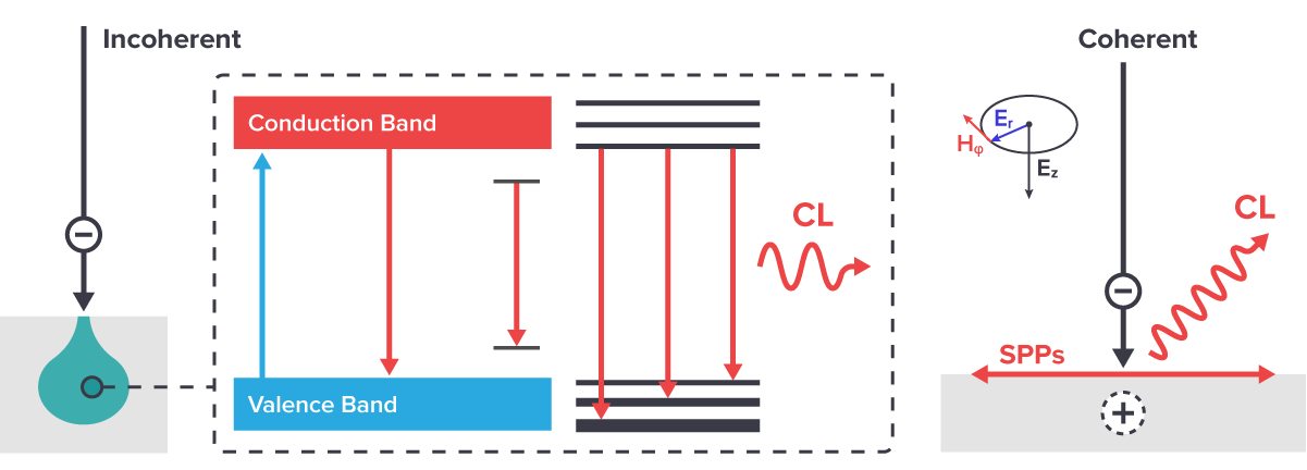 Figure 1: Incoherent and coherent CL emission. Incoherent CL occurs when an incoming electron deposits energy into the material, and subsequently a photon is emitted. Coherent CL occurs when the material is localy polarised due to incoming electrons, and strongly polarized light is emitted.
Gaining insights with cathodoluminescence
Now that we have covered CL emission itself, let’s take a closer look at the various research fields where CL is currently used and explore how this technique is helping researchers in answering their research questions.
CL imaging is widely used in the field of structural geology [1]. Researchers use CL to gain insights into the composition and history of diverse rocks, including zircons, sedimentary rocks, and meteorite impacts. CL can unveil small-scale details such as local defects, crystal zonation, impurities, and more. Frequently, it is combined with other techniques such as backscattered electron imaging (BSE) and energy-dispersive X-ray spectroscopy (EDS).
In semiconductor research, CL is instrumental in inspecting a wide variety of materials, ranging from perovskites for solar applications to gallium nitride (GaN) for LED applications, and transistorsfor power electronics. Primarily, CL is used to gain insights into the small-scale defects of materials and to probe local light emission. More specifically, CL can provide insights into material strain, carrier diffusion, point defects, homogeneity in optical response, and more. These detailed insights contribute to the design of materials with superior properties.
Related to this is the field of nanophotonics, where CL is used to study nanostructures such as nanowires, photonic crystals, and metasurfaces for applications such as LEDs and solar cells. CL can measure the local density of optical states and visualize the internal structure of nanostructures, which is crucial for understanding the optical properties of the material.
Quantum research also benefits from CL, as it is used to investigate the quantum mechanical properties of various materials, including 2D materials, quantum dots, and emitter centers, and investigate their local optical properties at the nanoscale.
The application of CL has expanded over the years, introducing new CL techniques and extending into novel fields of research such as correlative cathodoluminescence electron microscopy imaging (CCLEM) and the study of microplastics [2][3] (Figure 2).
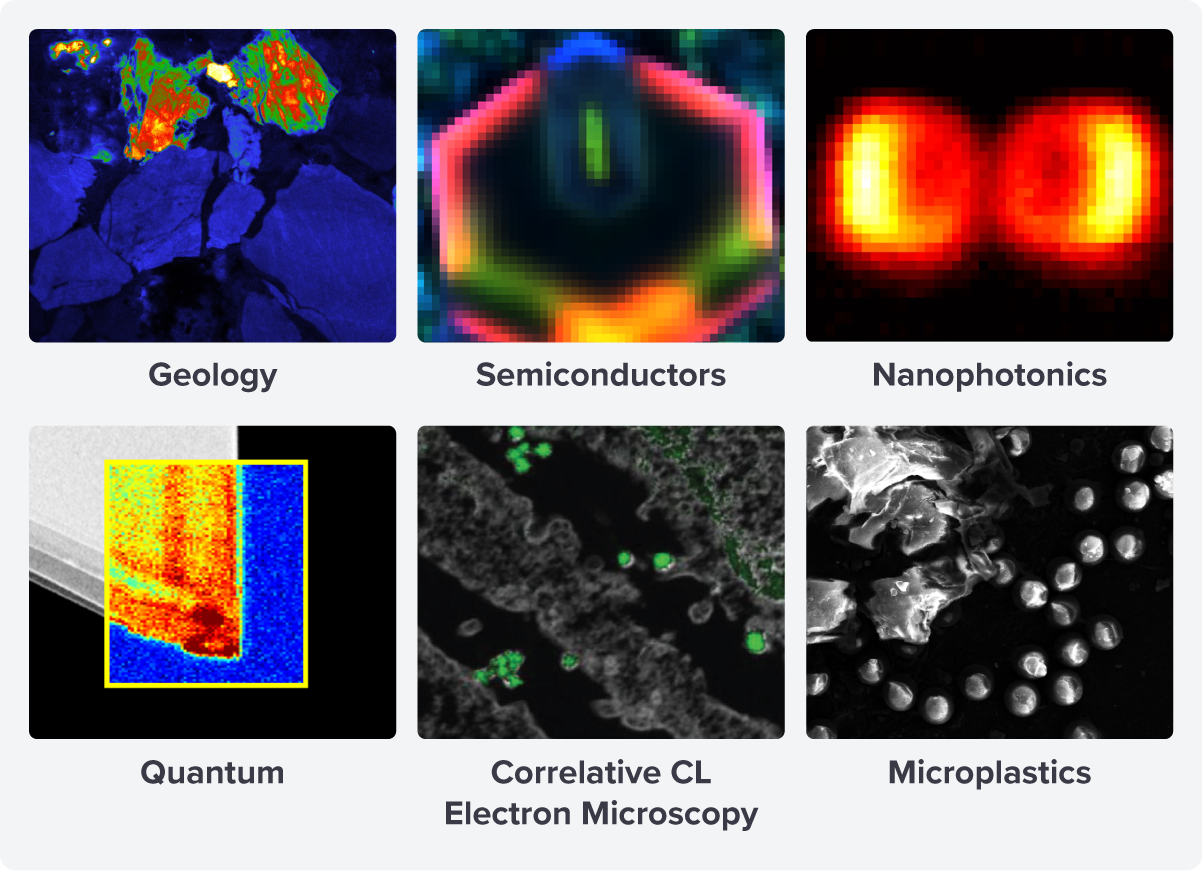 Figure 2: The application areas for cathodoluminescence imaging include geology, semiconductors, nanophotonics, quantum, CCLEM, and microplastics.
In the table below, we highlight some examples of materials and material types that have been studied using cathodoluminescence with corresponding references.
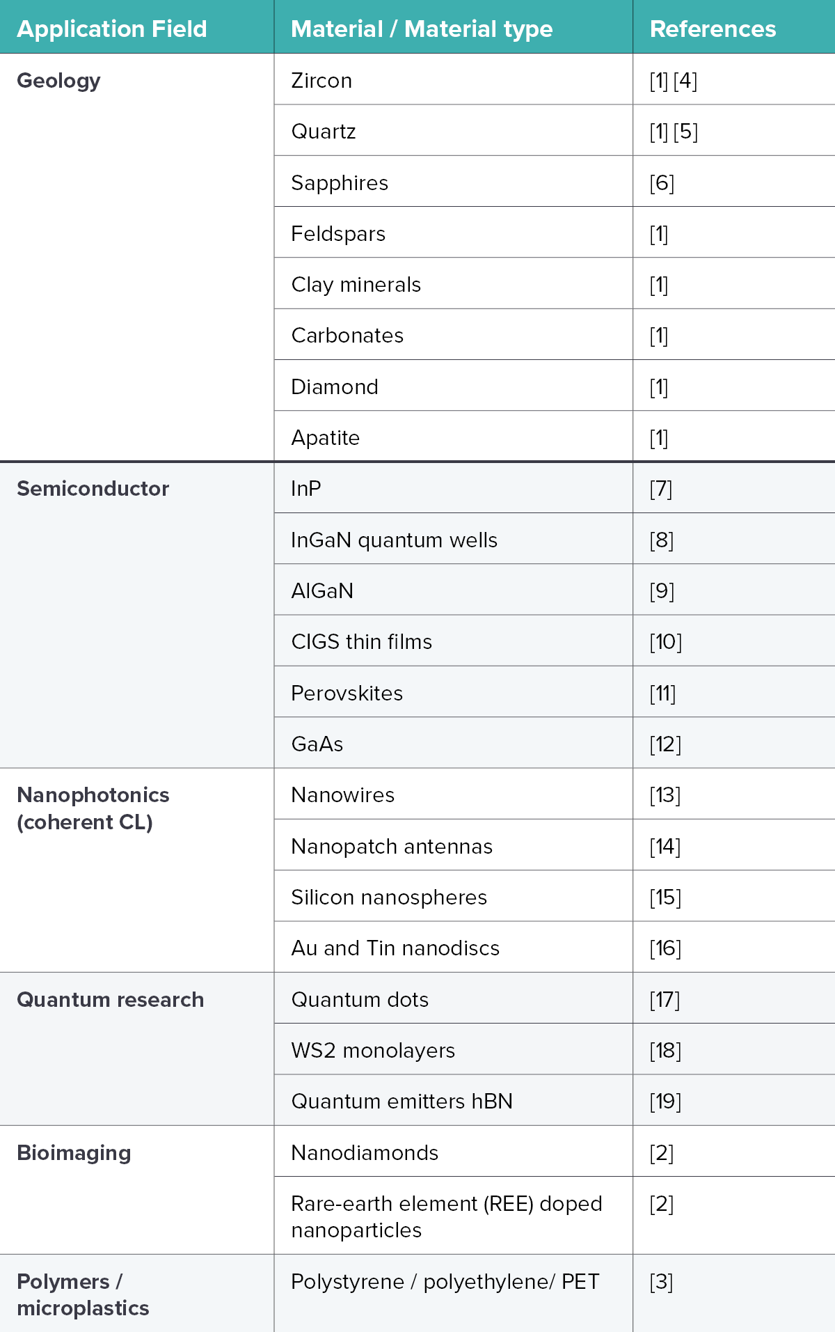
Table 1: Examples of materials imaged with CL from various application fields with corresponding references.
Cathodoluminescence imaging in an SEM
When these materials are imaged using CL, the material also has to be made suitable for imaging. Typically, CL imaging occurs in a scanning electron microscope (SEM), where the material is exposed to an electron beam in a vacuum environment. While imaging, the material receives an electron dose, so a conductive path to the ground is required to prevent charge buildup. For non-conductive samples, charging can be minimized by optimizing the beam parameters or adding a conductive layer to the sample.
Materials react differently to the electron beam, with some being more sensitive than others. This sensitivity can lead to damage and alterations to the sample during imaging, particularly in the case of polymers and organic tissues. Therefore, imaging conditions should be carefully chosen for these materials.
Another thing to keep in mind is that there are several different cathodoluminescence imaging techniques, each providing unique insights into materials. Beyond solely measuring CL intensity, researchers are also using techniques such as angle-resolved CL and time-resolved CL to measure the emission angle and time dynamics of a material, respectively. These techniques can enhance our understanding of materials even further.
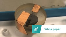
In summary, cathodoluminescence imaging proves to be an exceptionally versatile technique, enabling the study of optical properties in a diverse range of materials at the nanoscale. But how should you prepare your samples for cathodoluminescence imaging? Read it in our white paper below!
References
[1] Götze, J. et al., Microscopy and Microanalysis 18, 6, 1270–1284 (2012)
[2] Keevend et al., Nanoscale 12, 15588-15603 (2020)
[3] Höppener, E.M. et al., Talanta 253, 123985 (2023)
[4] Huijsmans, J.R. et al., Minerals 12, 1489 (2022)
[5] Delmic White Paper 'High-resolution Cathodoluminescence Spectroscopy on Shocked Quartz Grains'
[6] Delmic White Paper 'Complementary Cathodoluminescence and Mass Spectrometry of Australian Sapphires'
[7] Brenny, B.J.M. et al., Appl. Phys. Lett. 107, 201110 (2015)
[8] Meuret, S. et al., Phys. Rev. B 96, 3, 035308 (2017)
[9] Spende, H. et al., ACS Photonics, 9, 5, 1594–1604 (2022)
[10] Abou-Ras, D. et al., Phys. Status Solidi RRL 15, 2100042 (2021)
[11] Guthrey, H. et al., Adv. Energy Mater. 10, 1903840 (2020)
[12] Coenen, T. et al., Appl. Phys. Rev. 4 (3), 031103 (2017)
[13] Liu, A.C.Y. et al., Small 19, 2207747 (2023)
[14] Iyer, V. et al., APL Photonics 6 (10), 106103 (2021)
[15] Fiedler, S. et al., Nano Lett. 22, 6, 2320–2327 (2022)
[16] Bower, R. et al., Opt. Mater. Express 12, 3471-3479 (2022)
[17] Li, S. et al., ACS Photonics 10, 8, 2846–2853 (2023)
[18] Fiedler, S. et al., 2D Mater. 10, 021002 (2023)
[19] Gale, A. et al., ACS Photonics 9, 6, 2170–2177 (2022)