materials science
Nanophotonics insights: disentangling the CL spectrum
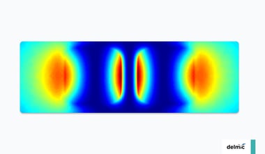
When measuring the optical response of silicon nanospheres using cathodoluminescence (CL), researchers found that interference can occur in the spectrum. Here, ...
.svg "DELMIC")
.png)
Acquire more powerful insights to progress your research
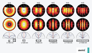
Resolve optical properties at the nanoscale


All topics
When measuring the optical response of silicon nanospheres using cathodoluminescence (CL), researchers found that interference can occur in the spectrum. Here, ...
Intensity mapping using cathodoluminescence (CL) emission is a powerful tool for high-resolution probing of emitters. The CL signal comes from both the UV ...
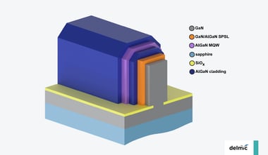
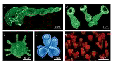
The advancement of nanotechnology opened up exciting new possibilities to create nanophotonic structures with nanoscale dimensions. A fundamental understanding ...

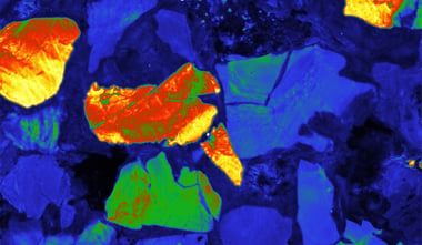
Understanding how different materials work and knowing their properties has been a keystone in human progress. In our efforts to build an environmentally ...

Are you interested in the possibilities of cathodoluminescence (CL) for photovoltaics (PV)?
If you are working in the field of photovoltaics or optoelectronics, you know that perovskites, a group of materials that have ABX3 composition and a ...
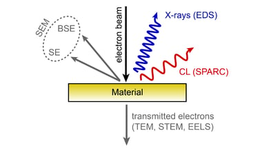
Those who understand the basic mechanisms of cathodoluminescence (CL) know that it is essentially a useful byproduct of electron microscopy.

In 1897, the electron was discovered by Sir Joseph John Thomson. The physicist and eventual Nobel Prize winner was in fact conducting research on “cathode ...