DELMIC
Delmic_Black+Blue(preferred)@2x(1)
Twitter-logo Linkedin-logo Youtube-logo
  • Life Sciences arrow image

    Delmic for life sciences

    Acquire more powerful insights to progress your research

    Explore solutions

    Our solutions

    • product-icon_METEOR METEOR
    • product-icon_FAST-EM FAST-EM
    • product-icon_CERES-IS CERES Ice Shield
    • product-icon_CERES-CS-VL CERES Sample Preparation
    • product-icon_SECOM SECOM

    Workflows

    • Cryo Electron Tomography
    • High-throughput EM
    • Correlative light EM

    Insights

    • Publications
    • Blog
    • Webinars
    • White papers
    • Application notes
    • Technical notes
  • Materials Analysis arrow image

    Delmic for materials analysis

    Resolve optical properties at the nanoscale

    Explore solutions

    Our solutions

    • product-icon_SPARC-Spectral SPARC Spectral
    • product-icon_SPARC Compact SPARC Compact
    • product-icon_JOLT JOLT 2.0
    • product-icon_LAB-Cube LAB Cube

    Techniques

    • Cathodoluminescence

    Applications

    • Geology
    • Semiconductors
    • Nanophotonics
    • Quantum

    Insights

    • Publications
    • Blog
    • Webinars
    • White papers
    • Application notes
    • Technical notes
  • Why Delmic?
  • Insights arrow image

    Insights

    • Blog
    • Customer stories
    • Resource library
    • Feed

    Technique Deep Dives

    • Cathodoluminescence
    • Cryo-electron tomography
    • High-throughput EM
    • Correlative light and electron microscopy
  • Company arrow image

    What do we do?

    We aspire to achieve seamless microscopy as the standard

    Learn more

    Company

    • About us
    • News
    • Career
    • Distributors
    • Contact
Search
Get in touch
Search
hamburger close

Blog

  • cathodoluminescence
  • life sciences
  • cryo electron microscopy
  • cryo-electron tomography
  • SPARC
  • materials science
  • fast SEM imaging
  • FAST-EM
  • geology
  • nanophotonics
  • correlative light and electron microscopy
  • semiconductors
  • SECOM
  • METEOR
  • cryo-focused ion beam
  • time-resolved cathodoluminescence
  • photovoltaics
  • software
  • volume electron microscopy
  • Array tomography
  • State of electron microscopy
  • plasmonics
  • History of microscopy
  • LAB Cube
  • Scanning electron microscope (SEM)
  • artificial intelligence
  • drug development
  • event
  • microplastics
  • power electronics
  • webinar
  • 冷冻电子断层扫描
  • All topics

cathodoluminescence
Studying UV LED materials with cathodoluminescence imaging

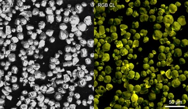
Cathodoluminescence is commonly used to probe light emission characteristics in semiconductor LED materials.

cathodoluminescence
What is the difference between coherent and incoherent cathodoluminescence?

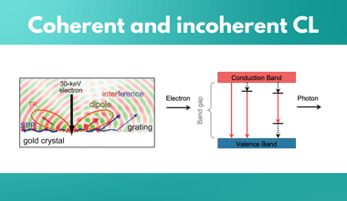
Cathodoluminescence processes can be divided into two categories: coherent and incoherent CL. But what is the difference between these? In this blog post we ...

cathodoluminescence
Observing defects in rocks using cathodoluminescence

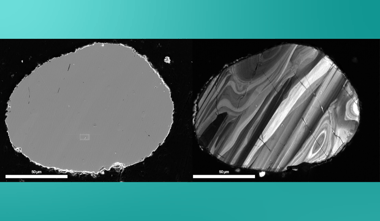
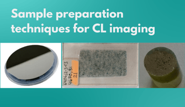
Cathodoluminescence is commonly used to pre-screen geological samples and combined with other SEM techniques for in-depth study. Various CL imaging modes can ...

cathodoluminescence
How to prepare your sample for cathodoluminescence imaging?

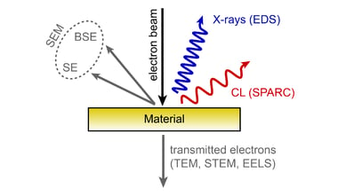
Cathodoluminescence is a specific form of luminescence caused by ‘free’ electrons (or simply electron propagating through space).

cathodoluminescence
How to study properties of rare-earth doped materials with cathodoluminescence

Rare-earth elements, also known as REE, are a group of elements, consisting of scandium, yttrium and 15 lanthanide elements.

cathodoluminescence
How can time-resolved cathodoluminescence imaging expand applications of (compound) semiconductors in new technologies?

Semiconductors, as a crucial part of electronic devices, have been in focus in materials research in the last few decades.

cathodoluminescence
How to perform lifetime imaging using time-resolved cathodoluminescence?

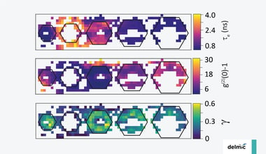
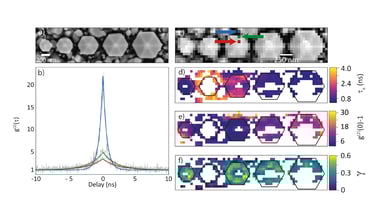
What is time-resolved cathodoluminescence? How can performing lifetime mapping or a g(2) mapping add value to your research? In the video below Toon Coenen, ...

cathodoluminescence
What are the optimal imaging conditions for cathodoluminescence?

Understanding the effects of the SEM parameters on generating (incoherent) cathodoluminescence (CL) is essential for obtaining high-quality CL intensity maps ...

cathodoluminescence
How can cathodoluminescence imaging modes enhance your research in 6 ways?

Cathodoluminescence is a great tool for obtaining valuable information about the properties of a sample, which can empower researchers and developers with a ...

materials science
What is the difference between cathodoluminescence and other SEM techniques?

materials science
How does cathodoluminescence for measuring photovoltaic materials work?

Are you interested in the possibilities of cathodoluminescence (CL) for photovoltaics (PV)?

cathodoluminescence
Best microscopy techniques for studying CIGS thin-film solar cells

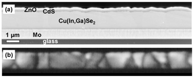
A copper indium gallium selenide (or CIGS), a direct bandgap semiconductor is being commonly used for solar cell production.

  • 2
  • 3
  • 4
  • →
Delmic_Black+Blue(preferred)@2x

Life science Frame 264(3)

Solutions
  • METEOR
  • FAST-EM
  • CERES Ice Shield
  • CERES Sample Preparation
  • SECOM
Workflows
  • Cryo Electron Tomography
  • High-throughput EM
  • Correlative light EM

Materials analysis Frame 264(3)

Solutions
  • SPARC Spectral
  • SPARC Compact
  • JOLT 2.0
  • LAB Cube
Techniques
  • Cathodoluminescence
Applications
  • Geology
  • Semiconductors
  • Nanophotonics
  • Quantum

Insights Frame 264(3)

  • Blog
  • Customer stories
  • Resource library
Deep dive
  • Cathodoluminescence
  • Cryo-EM
  • High-throughput EM
  • CLEM

Company Frame 264(3)

  • About Delmic
  • News
  • Distributors
  • Careers
  • Contact