
cathodoluminescence
Will lead-free Perovskite solar cells lead the future?
Perovskite solar cells could spur the growth of solar power, but they currently contain lead, which is toxic. Recently, scientists have started to explore ...
.svg "DELMIC")
.png)
Acquire more powerful insights to progress your research
Resolve optical properties at the nanoscale


All topics
Perovskite solar cells could spur the growth of solar power, but they currently contain lead, which is toxic. Recently, scientists have started to explore ...
When measuring the optical response of silicon nanospheres using cathodoluminescence (CL), researchers found that interference can occur in the spectrum. Here, ...

There is an increased need for Germanium (Ge), yet little is known about the properties of this scarce element. In this blog, we will discuss a novel paper ...
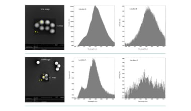
Intensity mapping using cathodoluminescence (CL) emission is a powerful tool for high-resolution probing of emitters. The CL signal comes from both the UV ...
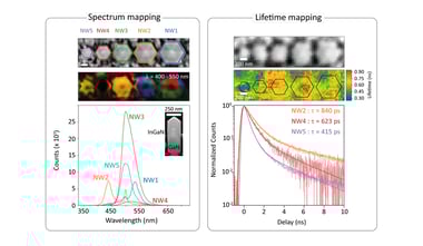
The advancement of nanotechnology opened up exciting new possibilities to create nanophotonic structures with nanoscale dimensions. A fundamental understanding ...

Understanding how different materials work and knowing their properties has been a keystone in human progress. In our efforts to build an environmentally ...

Geochronology plays a central role in geosciences and all historical aspects of the Earth sciences. Over the years, it has become an essential scientific field ...
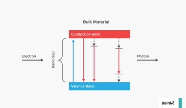
Cathodoluminescence (CL) is the process of light emission from a material as a result of excitation by electrons. Imaging CL can therefore enable us to study ...
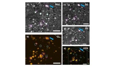
In the past few years, cathodoluminescence (CL) has become more widely used in various fields, including geology, nanophotonics, materials science and even ...
As a powerful technique with high spatial resolution, cathodoluminescence (CL) imaging has been applied in many different fields, from geology to nanophotonics ...
Understanding the relationship between structure and function in biology relies strongly on imaging. While correlative light and electron microscopy (CLEM) is ...
Cathodoluminescence imaging is a powerful technique often used to investigate semiconductor materials.