.svg "DELMIC")
.png)


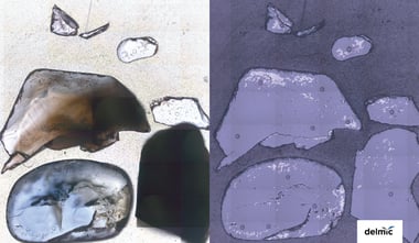
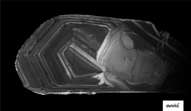
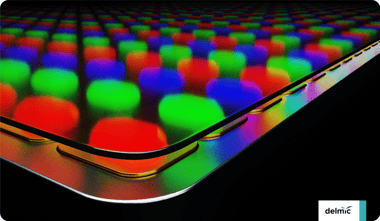
cathodoluminescence
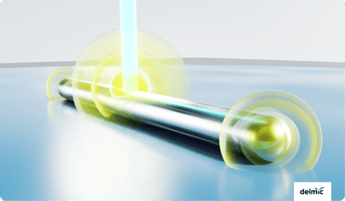
High-resolution Cathodoluminescence for semiconductor nanostructures
In the realm of nanotechnology, studying thermal properties at the nanoscale is crucial for understanding and improving the efficiency and sensitivity of devices. As integrated electronic circuits...